Continuous Integration Multi slope Iii a d Converter
In this tutorial, we will discuss slope type or integration type ADC. In the last tutorial, we have discussed successive approximation and Flash type ADC. There are two types of slope ADCs such as single slope and dual slope. Firstly, we will discuss single slope and after that, we will see the working of dual-slope integration ADC.
Slope Type ADC Introduction
Single and dual slope ADCs are the types that digitize the analog signals using integrated circuits and integrated circuits are designed using operational amplifiers. In this type, we generate a sawtooth waveform using an op-amp as an integrator. The output of sawtooth waveform is compared against the analog input using a comparator circuit to generator a digital output.
They have a high resolving power but are quite slower in terms of conversion speed than other analog to digital converters. Its major application is in the multimeter. The article shares the working of single and dual ADCs, benefits, downsides, and applications.
Single slope ADC (Integrated ADC )
Dual slope ADC is preferred over the single slope analog to digital converter. For a clear conception of the dual-slope ADC, we will study the single slope first. It consists of an integrator and a comparator.
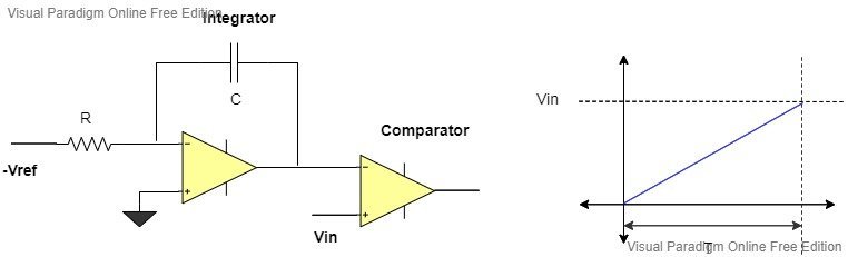
The input voltage is applied to the positive terminal of the comparator while the reference voltage is obtained after being integrated through the integrator. Both of the voltages get compared through the comparator. The input voltage is a function of time t. The reference voltage keeps on integrated until the output voltage of the comparator becomes equal to the input voltage.
The general output voltage of the integrator is given as
VO=1/RC (-Vref) dt
In the equation, we can see that the reference voltage is negative, so the slope of the integrated output voltage turns out to be positive.
The output voltage of the integrator at any given time is given as
VO=T*Vref/RC
At time T, the output voltage is equivalent to the input voltage. So, we can say
Vin=T*Vref/RC
As the reference voltage, resistor R, and capacitor C are fixed for a given analog to digital converter, the input voltage is directly proportional to time.
Schematic diagram
Below is the schematic diagram of a single slope analog to digital converter:

It consists of an integrator, a comparator, an AND gate, and a counter that gives us the binary outputs. The output of the comparator is passed to the AND gate. Whenever the output of the comparator is high which means that when the reference voltage is lesser than the input voltage, clock pulses are given to the counter through the AND gate, and the counter starts counting.
Working Principle
Before converting the analog input into binary output, the counter is reset to zero. The input voltage and an integrated reference voltage are applied to the comparator. When the conversion begins, initially the reference voltage is less than the input voltage. The output of the comparator is high and because of this, the counter receives clock pulses, and the counter works and counts. So, when the integrated reference voltage becomes equal to the applied input voltage, the comparator changes its state from high to low. The output of the AND gate becomes low, the counter no longer gets any clock pulses and stops the count. Whatever, the count is then available on the counter will be proportional to the input voltage.
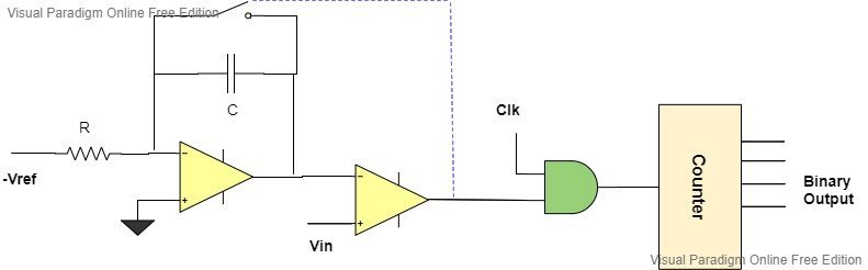
The circuit is also accompanied by a switch known as Reset Switch. It gets closed shortly when the comparator's output is low and makes sure that there is no leftover charge across the capacitor to avoid any errors. This is the process through which the single slope analog to digital converter transforms the given analog signal to the digital output signal.
Graphical Representation
The graphical representation depicts the effect on input voltage and resistance on the graph.
Relation of Vin and T.
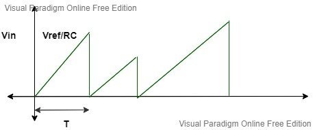
The above graph shows the time taken for the integration with respect to the applied input voltage. The reference voltage and RC are constant that is why the slope i.e. Vref/RC is constant. The input voltage only affects the time. Higher the input voltage, more time will be taken for the integration process while the slope remains the same.
As clear from the graph this ADC has a single slope which leads to its name as Single slope ADC.
Effect of RC
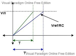
If the input voltage is fixed and R or C changes then the slope changes. Despite a constant input, we will achieve a different time of integration. Let's say if the R value is reduced then the time taken by the integrator circuit to reach the input voltage in magnitude will get less as well.
This value of RC changes with time due to external factors like temperature etc which is a major reason for its poor accuracy and leads us to its solution which is a dual-slope analog to digital converter.
Dual Slope ADC
The integrator of a dual-slope analog to digital converter has a switch at its input side which can either connect to a reference voltage or an input voltage. Initially in the conversion, the switch is connected to the input voltage and the integrator integrates the input voltage until its output equals the applied voltage.
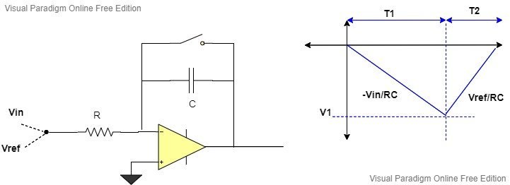
If the output voltage is V1 and T1 is the time taken then the V1 is given as:
VO= -1/RC Vin dt V1= -T1*Vin/RC
After T1 time, the switch gets connected to the reference voltage and the respective voltage is integrated. The diagram shows that the given reference voltage is negative yet it is usually greater than the input voltage.
As negative reference is applied, the integrator integrates in a positive direction and keeps on integrating until the output is equal to the zero voltage. The time taken is represented by T2.
After time T1, the integrator's output is
VO= -1/RC -Vref dt + Vinitial
Which for time T2 can be written as
VO= -T2*(-Vref)/RC + V1
Where V1 is the initial voltage across the capacitor and VO is the total output voltage across the integrator in total time T1+T2.
If we replace V1 by its value in the above equation then
VO= T2*(Vref)/RC +(-T1*Vin/RC)
The output would be equal to zero after T1+T2. The equation becomes
T2*(Vref)/RC +(-T1*Vin/RC)=0 T2=T1*Vin/Vref
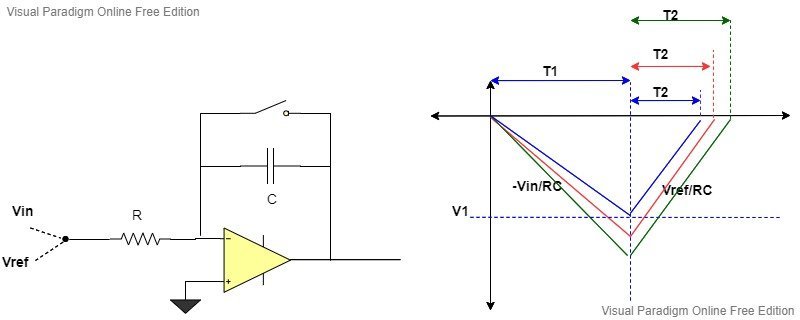
In dual-slope ADC, T1 and reference voltage are constant which gives the result that the time T2 is directly proportional to the input voltage. If the input voltage changes, T2 also changes. This is represented through the graph below.
Dual slope Working Principle
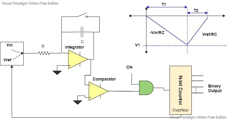
The integrator's output is connected to the negative terminal of the comparator and the positive terminal of the comparator is connected to the ground. At the start of the conversion, the input voltage is connected to the integrator. The integrator integrates it in the negative direction. When compared with the ground, the inverting terminal is negative with respect to the non-inverting terminal so the output of the comparator becomes high. Just like the single slope, the AND signal then provides the clock pulses to the n-bit counter and starts counting from zero onwards until overflow becomes 1. The counter takes 2^N clocks to integrate the input signal.
When the overflow is detected, the switch automatically toggles and joins with the negative reference voltage. As the reference voltage is negative, the integrator begins integrating in the positive direction and the same procedure is repeated. This time the counter will stop counting when the output of the comparator gets low. At that particular time, the binary output of the n-bit counter would be directly proportional to the time T2. In this way, the dual-slope ADC does the conversion.
The total conversion time of this ADC is given by
Ttotal= 2^N*Tc + T2 Ttotal= 2^N*Tc + N*Tc
Where Tc is the clock duration.
If both slopes are equal or we say the input voltage is the same as the reference voltage, the total time becomes
2^(N+1)*Tc
Advantages
- It provides better noise immunity than other ADC types.
- It also has good accuracy.
- The input signal is averaged.
Disadvantages
- The accuracy demands highly precise external components.
- The ADC slows down with the increase in the resolution that is why it is not used in data acquisition.
Applications
- Temperature Transducers
- Digital multimeters
Related Articles:
- R-2R Ladder DAC – Explained with Example Circuit Diagram
- ADC STM32F4 Discovery
- Binary Weighted Resistor DAC
- ADC TM4C123G Tiva C Launchpad
- PIC Microcontroller ADC
- Display ADC value on 4-digit 7-Segment Display using Pic Microcontroller
- HX711 24-Bit Analog-to-Digital Converter (ADC) for Weigh Scales
- ICL7107 ADC Display Driver
- ADC0804 ADC
- ADS1115 I2C external ADC with ESP32 in Arduino IDE
cardillomigniver91.blogspot.com
Source: https://microcontrollerslab.com/single-dual-slope-adc-integrating-analog-to-digital-converter/
0 Response to "Continuous Integration Multi slope Iii a d Converter"
Enviar um comentário